
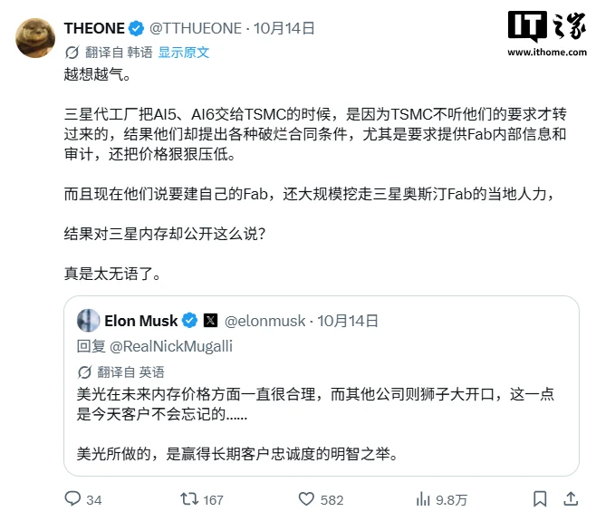
IT Home On October 18, according to Tweaktown reports, a South Korean semiconductor engineer claimed that when Tesla signed a chip foundry agreement with Samsung, it tried to obtain extremely favorable terms: both sensitive manufacturing process information and audit rights, while also demanding lower prices. The engineer, who posted on the X platform account @TTHUEONE, said that Tesla’s Terafab project has laid off many employees from Samsung’s factory in Tyler, Texas.
Before these allegations emerged, Elon Musk had just gone through a busy week. He publicly praised photonics technology, saying that it “has a rational approach to pricing future memory chips, while other manufacturers charge exorbitant prices.” These remarks were generally interpreted as a hint at Samsung. He also suggested that TSMC might be involved in the Terafab project – a major semiconductor project collaboration between Tesla and SpaceX – but ruled out the possibility of TSMC holding shares or participating in operations.
IT Home has noticed that the claim about talent being poached is not new. A report by The Business Post in March this year pointed out that the two factories are located close to each other, posing a structural risk to Samsung. It mentioned that Terafab will compete for labor and supplier resources in the same area. At that time, Tesla was already recruiting semiconductor R&D engineers for this project.
Recently, it was reported that Samsung has dispatched engineers specializing in advanced process yields from South Korea to the Taylor factory to fill staff gaps, in preparation for the mass production of 2-nanometer chips planned to start in 2027.
Regarding the chip foundry contract at the core of the dispute, Tesla’s AI5 chip has been trial-produced at Samsung Taylor Factory, with mass production targeted for 2027. The design of this chip is approximately half-mask size, featuring a large bare computing die in the center, surrounded by 12 memory modules, and its computing power target is 2000 to 2500 TOPS.
Musk said the chip’s performance is about three times that of Nvidia chips of the same level, and its cost is only one tenth of the latter. However, these figures have not yet been independently verified by third parties. The AI6 and AI6.5 chips are expected to use TSMC and Samsung’s 2-nanometer process, respectively. The on-chip static random memory capacity will be significantly increased, with the memory capacity reduced to 144GB.
Neither Tesla nor Samsung have confirmed or denied the allegations against this engineer. This incident also highlights that, in the AI computing power race, the conflicts in the semiconductor supply chain between chip designers and wafer manufacturers are intensifying.